- 您现在的位置:买卖IC网 > Sheet目录1917 > DSPIC30F4011-30I/ML (Microchip Technology)IC DSPIC MCU/DSP 48K 44QFN
dsPIC30F4011/4012
DS70135G-page 12
2010 Microchip Technology Inc.
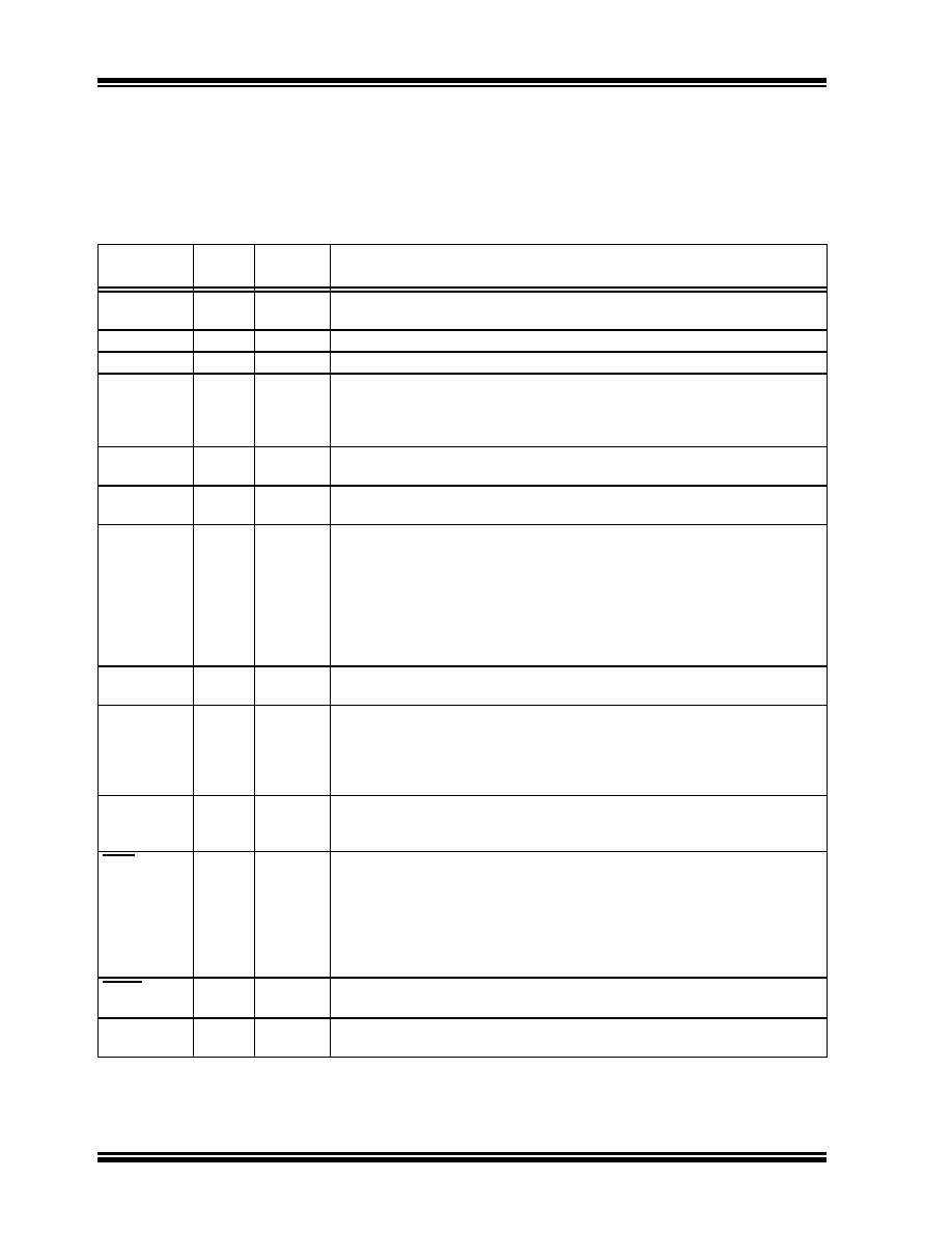
Table 1-1 provides a brief description of the device I/O
pinout and the functions that are multiplexed to a port
pin. Multiple functions may exist on one port pin. When
multiplexing occurs, the peripheral module’s functional
requirements may force an override of the data
direction of the port pin.
TABLE 1-1:
dsPIC30F4011 I/O PIN DESCRIPTIONS
Pin Name
Pin
Type
Buffer
Type
Description
AN0-AN8
I
Analog
Analog input channels. AN0 and AN1 are also used for device programming
data and clock inputs, respectively.
AVDD
P
Positive supply for analog module. This pin must be connected at all times.
AVSS
P
Ground reference for analog module. This pin must be connected at all times.
CLKI
CLKO
I
O
ST/CMOS
—
External clock source input. Always associated with OSC1 pin function.
Oscillator crystal output. Connects to crystal or resonator in Crystal
Oscillator mode. Optionally functions as CLKO in RC and EC modes.
Always associated with OSC2 pin function.
CN0-CN7
CN17-CN18
I
ST
Input change notification inputs. Can be software programmed for internal
weak pull-ups on all inputs.
C1RX
C1TX
I
O
ST
—
CAN1 bus receive pin.
CAN1 bus transmit pin.
EMUD
EMUC
EMUD1
EMUC1
EMUD2
EMUC2
EMUD3
EMUC3
I/O
ST
ICD Primary Communication Channel data input/output pin.
ICD Primary Communication Channel clock input/output pin.
ICD Secondary Communication Channel data input/output pin.
ICD Secondary Communication Channel clock input/output pin.
ICD Tertiary Communication Channel data input/output pin.
ICD Tertiary Communication Channel clock input/output pin.
ICD Quaternary Communication Channel data input/output pin.
ICD Quaternary Communication Channel clock input/output pin.
IC1, IC2, IC7,
IC8
I
ST
Capture inputs 1, 2, 7 and 8.
INDX
QEA
QEB
I
ST
Quadrature Encoder Index Pulse input.
Quadrature Encoder Phase A input in QEI mode.
Auxiliary Timer External Clock/Gate input in Timer mode.
Quadrature Encoder Phase B input in QEI mode.
Auxiliary Timer External Clock/Gate input in Timer mode.
INT0
INT1
INT2
I
ST
External interrupt 0.
External interrupt 1.
External interrupt 2.
FLTA
PWM1L
PWM1H
PWM2L
PWM2H
PWM3L
PWM3H
I
O
ST
—
PWM Fault A input.
PWM1 low output.
PWM1 high output.
PWM2 low output.
PWM2 high output.
PWM3 low output.
PWM3 high output.
MCLR
I/P
ST
Master Clear (Reset) input or programming voltage input. This pin is an
active-low Reset to the device.
OCFA
OC1-OC4
I
O
ST
—
Compare Fault A input (for Compare channels 1, 2, 3 and 4).
Compare outputs 1 through 4.
Legend: CMOS =
CMOS compatible input or output
Analog =
Analog input
ST
=
Schmitt Trigger input with CMOS levels
O
=
Output
I
=
Input
P
=
Power
发布紧急采购,3分钟左右您将得到回复。
相关PDF资料
DSPIC30F4013-30I/ML
IC DSPIC MCU/DSP 48K 44QFN
DSPIC30F5013-30I/PT
IC DSPIC MCU/DSP 66K 80TQFP
DSPIC30F5015-30I/PT
IC DSPIC MCU/DSP 66K 64TQFP
DSPIC30F6010-20E/PF
IC DSPIC MCU/DSP 144K 80TQFP
DSPIC30F6010A-30I/PF
IC DSPIC MCU/DSP 144K 80TQFP
DSPIC30F6013A-30I/PF
IC DSPIC MCU/DSP 132K 80TQFP
DSPIC30F6014-30I/PF
IC DSPIC MCU/DSP 144K 80TQFP
DSPIC33EP512MU814-I/PL
IC DSC 16BIT 512KB 144LQFP
相关代理商/技术参数
DSPIC30F4011-30I/P
功能描述:数字信号处理器和控制器 - DSP, DSC 16bit Signal Cntrlr RoHS:否 制造商:Microchip Technology 核心:dsPIC 数据总线宽度:16 bit 程序存储器大小:16 KB 数据 RAM 大小:2 KB 最大时钟频率:40 MHz 可编程输入/输出端数量:35 定时器数量:3 设备每秒兆指令数:50 MIPs 工作电源电压:3.3 V 最大工作温度:+ 85 C 封装 / 箱体:TQFP-44 安装风格:SMD/SMT
DSPIC30F4011-30I/PT
功能描述:数字信号处理器和控制器 - DSP, DSC 16 Bit MCU/DSP 30M 48KB FL RoHS:否 制造商:Microchip Technology 核心:dsPIC 数据总线宽度:16 bit 程序存储器大小:16 KB 数据 RAM 大小:2 KB 最大时钟频率:40 MHz 可编程输入/输出端数量:35 定时器数量:3 设备每秒兆指令数:50 MIPs 工作电源电压:3.3 V 最大工作温度:+ 85 C 封装 / 箱体:TQFP-44 安装风格:SMD/SMT
DSPIC30F4011T-20E/ML
功能描述:数字信号处理器和控制器 - DSP, DSC 16 Bit MCU/DSP 44LD 20M 48KB FL RoHS:否 制造商:Microchip Technology 核心:dsPIC 数据总线宽度:16 bit 程序存储器大小:16 KB 数据 RAM 大小:2 KB 最大时钟频率:40 MHz 可编程输入/输出端数量:35 定时器数量:3 设备每秒兆指令数:50 MIPs 工作电源电压:3.3 V 最大工作温度:+ 85 C 封装 / 箱体:TQFP-44 安装风格:SMD/SMT
DSPIC30F4011T-20E/PT
功能描述:数字信号处理器和控制器 - DSP, DSC 16 Bit MCU/DSP 20M 48KB FL RoHS:否 制造商:Microchip Technology 核心:dsPIC 数据总线宽度:16 bit 程序存储器大小:16 KB 数据 RAM 大小:2 KB 最大时钟频率:40 MHz 可编程输入/输出端数量:35 定时器数量:3 设备每秒兆指令数:50 MIPs 工作电源电压:3.3 V 最大工作温度:+ 85 C 封装 / 箱体:TQFP-44 安装风格:SMD/SMT
DSPIC30F4011T-20I/ML
功能描述:数字信号处理器和控制器 - DSP, DSC DIG SIG CONTR RoHS:否 制造商:Microchip Technology 核心:dsPIC 数据总线宽度:16 bit 程序存储器大小:16 KB 数据 RAM 大小:2 KB 最大时钟频率:40 MHz 可编程输入/输出端数量:35 定时器数量:3 设备每秒兆指令数:50 MIPs 工作电源电压:3.3 V 最大工作温度:+ 85 C 封装 / 箱体:TQFP-44 安装风格:SMD/SMT
DSPIC30F4011T-20I/PT
功能描述:数字信号处理器和控制器 - DSP, DSC 16 Bit MCU/DSP 20M 48KB FL RoHS:否 制造商:Microchip Technology 核心:dsPIC 数据总线宽度:16 bit 程序存储器大小:16 KB 数据 RAM 大小:2 KB 最大时钟频率:40 MHz 可编程输入/输出端数量:35 定时器数量:3 设备每秒兆指令数:50 MIPs 工作电源电压:3.3 V 最大工作温度:+ 85 C 封装 / 箱体:TQFP-44 安装风格:SMD/SMT
DSPIC30F4011T-30I/ML
功能描述:数字信号处理器和控制器 - DSP, DSC 16 Bit MCU/DSP 44LD 30M 48KB FL RoHS:否 制造商:Microchip Technology 核心:dsPIC 数据总线宽度:16 bit 程序存储器大小:16 KB 数据 RAM 大小:2 KB 最大时钟频率:40 MHz 可编程输入/输出端数量:35 定时器数量:3 设备每秒兆指令数:50 MIPs 工作电源电压:3.3 V 最大工作温度:+ 85 C 封装 / 箱体:TQFP-44 安装风格:SMD/SMT
DSPIC30F4011T-30I/PT
功能描述:数字信号处理器和控制器 - DSP, DSC 16 Bit MCU/DSP 30M 48KB FL RoHS:否 制造商:Microchip Technology 核心:dsPIC 数据总线宽度:16 bit 程序存储器大小:16 KB 数据 RAM 大小:2 KB 最大时钟频率:40 MHz 可编程输入/输出端数量:35 定时器数量:3 设备每秒兆指令数:50 MIPs 工作电源电压:3.3 V 最大工作温度:+ 85 C 封装 / 箱体:TQFP-44 安装风格:SMD/SMT